| |
|
|
|
|
|
|
|
|
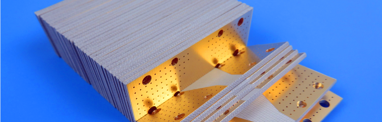
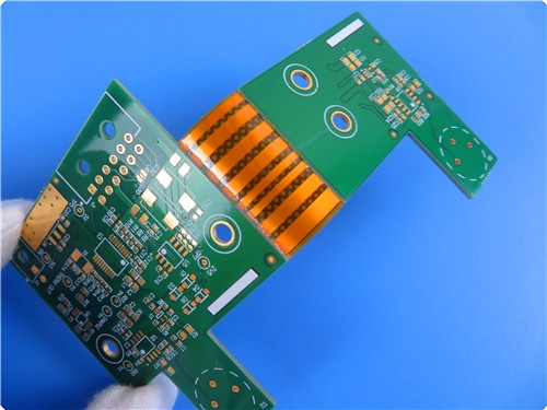
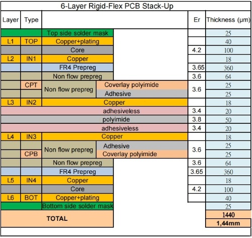
6 Layer Rigid Flex PCB Built on FR 4 and Polyimide With Immersion Gold and 90ohm Impedance Control from Shengyi |
|
|
(Printed Circuit Boards are custom-made products. The picture and parameters shown are for reference only.) |
|
|
|
|
|
General description |
|
|
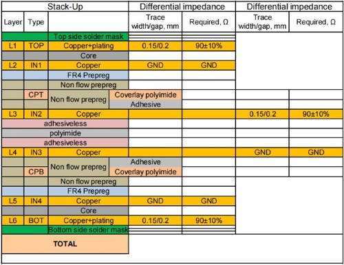
FR-4 and poyimide rigid-flexible printed circuit board is specifically designed for automotive GPS tracking devices, featuring a 6-layer construction with a total thickness of 1.4mm. The inner layers utilize half-ounce copper foil, while the outer layers employ 1-ounce copper. The design incorporates impedance-controlled routing on both the outer layers and the internal flexible circuitry to ensure signal integrity. Immersion gold plating is applied to the pads to facilitate surface mount technology (SMT) assembly. Constructed with a base laminate from Shengyi, this PCB is manufactured in strict accordance with IPC 6012 Class 2 standards using the provided Gerber files, guaranteeing reliable performance and adherence to industry specifications. |
|
|
|
|
|
 |
|
|
|
|
|
Basic specifications |
|
|
Size of Flexible PCB |
120.61 X 50.17mm |
Number of Layers |
6 |
Board Type |
Rigid-flex PCB |
Board Thickness |
1.44mm |
Board Material |
FR-4 / Polyimide |
Board Material Supplier |
Shengyi |
Tg Value of Board Material |
170℃ |
|
PTH Cu thickness |
≥20 µm |
Inner Iayer Cu thicknes |
18 µm |
Surface Cu thickness |
35 µm |
|
|
Coverlay Colour |
Yellow coverlay / Green solder mask |
Number of Coverlay |
2 |
Thickness of Coverlay |
25 µm |
Stiffener Material |
N/A |
Stiffener Thickness |
N/A |
|
|
Type of Silkscreen Ink |
IJR-4000 MW300 |
Supplier of Silkscreen |
TAIYO |
Color of Silkscreen |
White |
Number of Silkscreen |
1 |
|
Peeling test of Coverlay |
No peelable |
Legend Adhesion |
3M 90℃ No peeling after Min. 3 times test |
|
Surface Finish |
Immersion Gold |
Thickness of Surface Finish |
Au: 0.03µm(Min.); Ni 2-4µm |
RoHS Required |
Yes |
Famability |
94-V0 |
|
Thermal Shock Test |
Pass, -25℃±125℃, 1000 cycles. |
Thermal Stress |
Pass, 300±5℃,10 seconds, 3 cycles. No delamination, no blistering. |
Function |
100% Pass electrical test |
Workmanship |
Compliance with IPC-A-600H & IPC-6013C Class 2 |
|
|
|
|
|
|
 |
|
|
|
|
|
 |
|
|
|
|
|
Features and benefits |
|
|
Excellent flexibility
Reducing the volume
Weight reduction
Consistency of assembly
Increased reliability
The end can be whole soldered
Low cost
Continuity of processing
No minimum order quantity and low cost sample.
Make delivery on time. We keep higher than 98% on-time-delivery rate. |
|
|
|
|
|
Applications |
|
|
Contact belt of inkjet printer, industrial surveying and mapping instrument, Tablet PC camera soft board |
|
|
|
|
|
Processes |
|
|
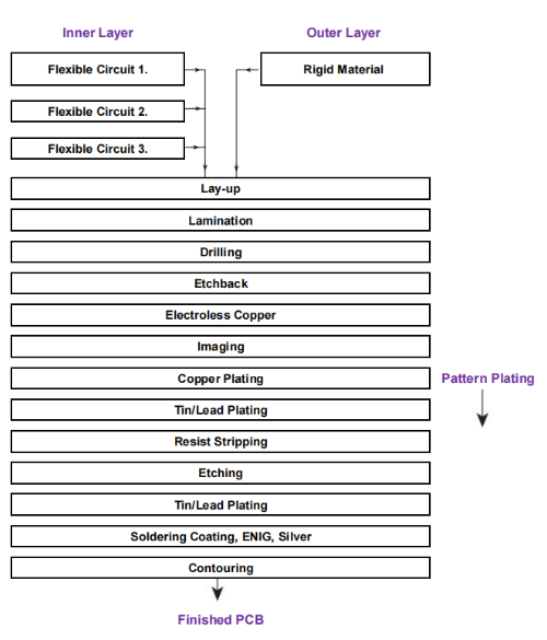
A simplified flow diagram is shown below. |
|
|
 |
|
|
|
|
|
Multilayer Flexible Circuits and Rigid-Flex PCBs |
|
|
Flexible Inner Layers |
|
|
The fabrication of inner layers in this rigid-flex PCB involves forming single- or double-sided flexible circuits through a standardized process: they undergo imaging, etching, and covering, yet drilling and plating are omitted. A distinct feature lies in the covercoating application for these inner layers, which includes an additional step to mitigate the risk of air pockets during processing.
When bonding the inner layers within the flexible section, this approach streamlines the manufacturing workflow by reducing procedural steps. However, the bonded structure results in a comparatively rigid circuit, limiting its bending capability. Specifically, this design typically allows a maximum of only 25 bend cycles before structural integrity is compromised.
Conversely, leaving the flexible circuits in the flex region unbonded offers an alternative. In scenarios where multiple inner layers exist or the rigid segments of the rigid-flex PCB are closely spaced, a staggered layer configuration can be implemented. This method helps prevent individual layer buckling when the circuit is bent into its operational form, though it introduces complexity to the manufacturing process due to the precise alignment required. |
|
|
|
|
|
Rigid Outer Layers |
|
|
In the manufacturing of rigid-flex circuits, rigid materials like FR-4 are precision-cut to specification and integrated into the circuit structure through the lamination process. To enhance handling during production, assembly, and soldering phases, the rigid-flex circuit can be temporarily manufactured as a fully rigid board by extending the rigid layers across the flexible section. To prevent the rigid outer layers from adhering to the flexible area, both surfaces of the flexible region are shielded with release films during lamination.
A critical step involves pre-cutting grooves along the edges of each rigid outer layer before lamination. This preparation allows for the subsequent removal of unbonded rigid material segments using a snap-action technique. By strategically designing these grooves at the interfaces of the rigid layers, the non-bonded portions can be efficiently separated, ensuring the final rigid-flex circuit maintains its intended flexibility in the designated areas while preserving structural integrity in the rigid sections. |
|
|
|
|
|
|
|
|
|
|
|
Hot Tags:
90ohm Impedance Control PCB |
Shengyi Tg170 FR-4 Laminate |
6-Layer FR-4 and Polyimide |
1.4mm Rigid Flex PCB |
Tg170 FR-4 Substrate |
|
|
|